
Code: DB313
Designed around the RP5C01 RTC chip, this kit gives your system the ability to remember the date and time when power is off. Its powered offline with a CR2450 battery.
In addition to keeping time, it also has a small amount of onboard RAM, that is also powered by the battery when main power is off. This RAM can be used to store machine specific settings, such as boot screen color and mode.
It also includes a reliable power-on-reset feature, sending RESET signal to your CPU when power is first applied.
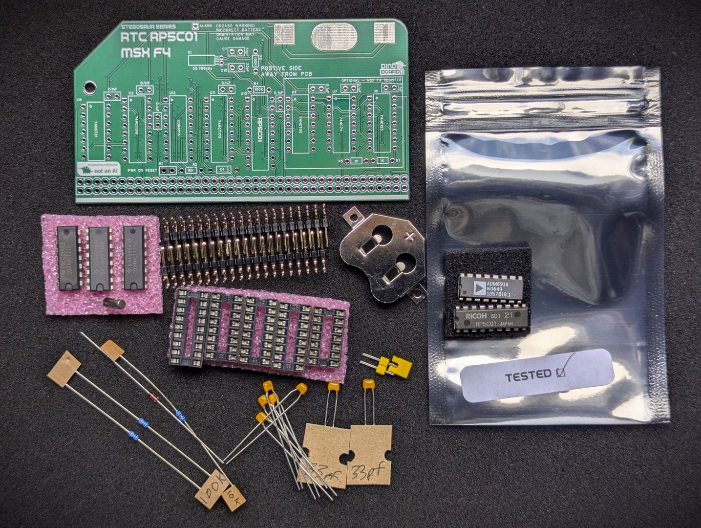 Kit Parts |
|
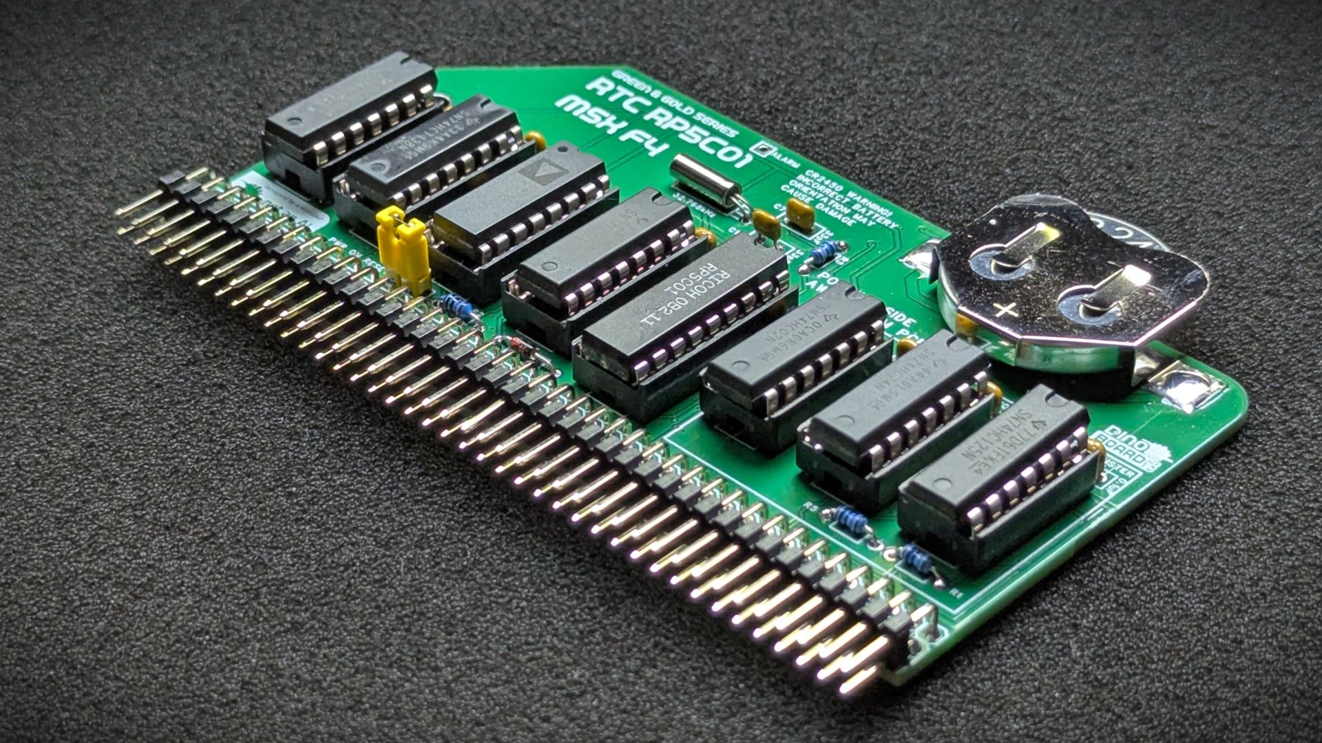
 Assembled Kit |
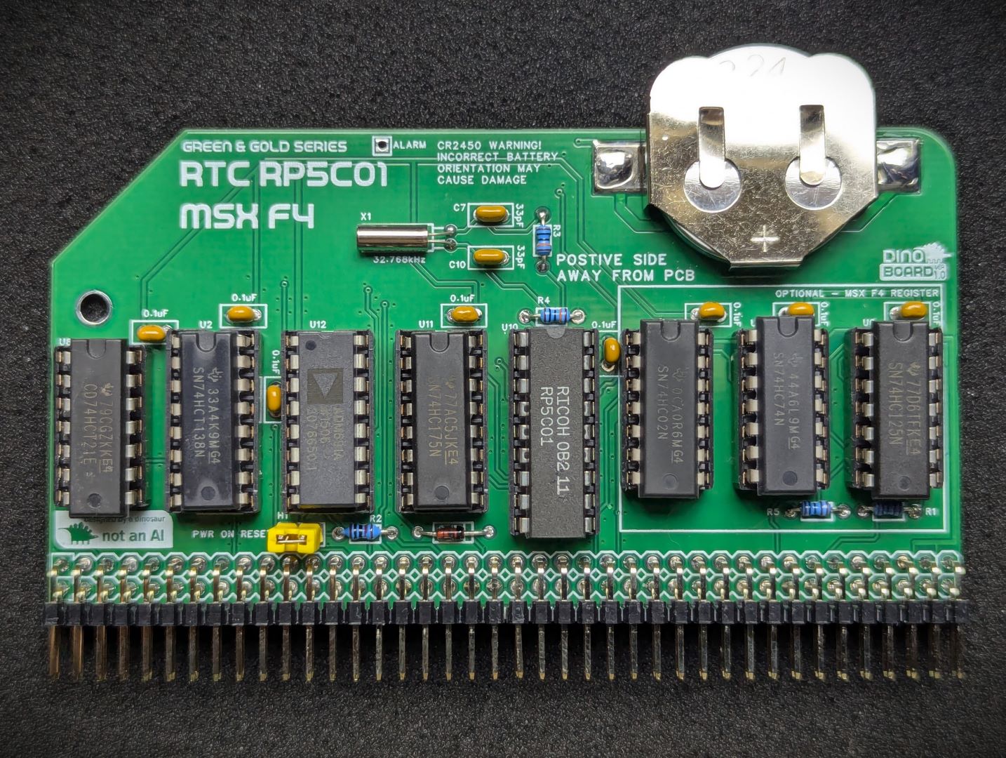
 Assembled Kit (without MSX F4 Boot Register) |
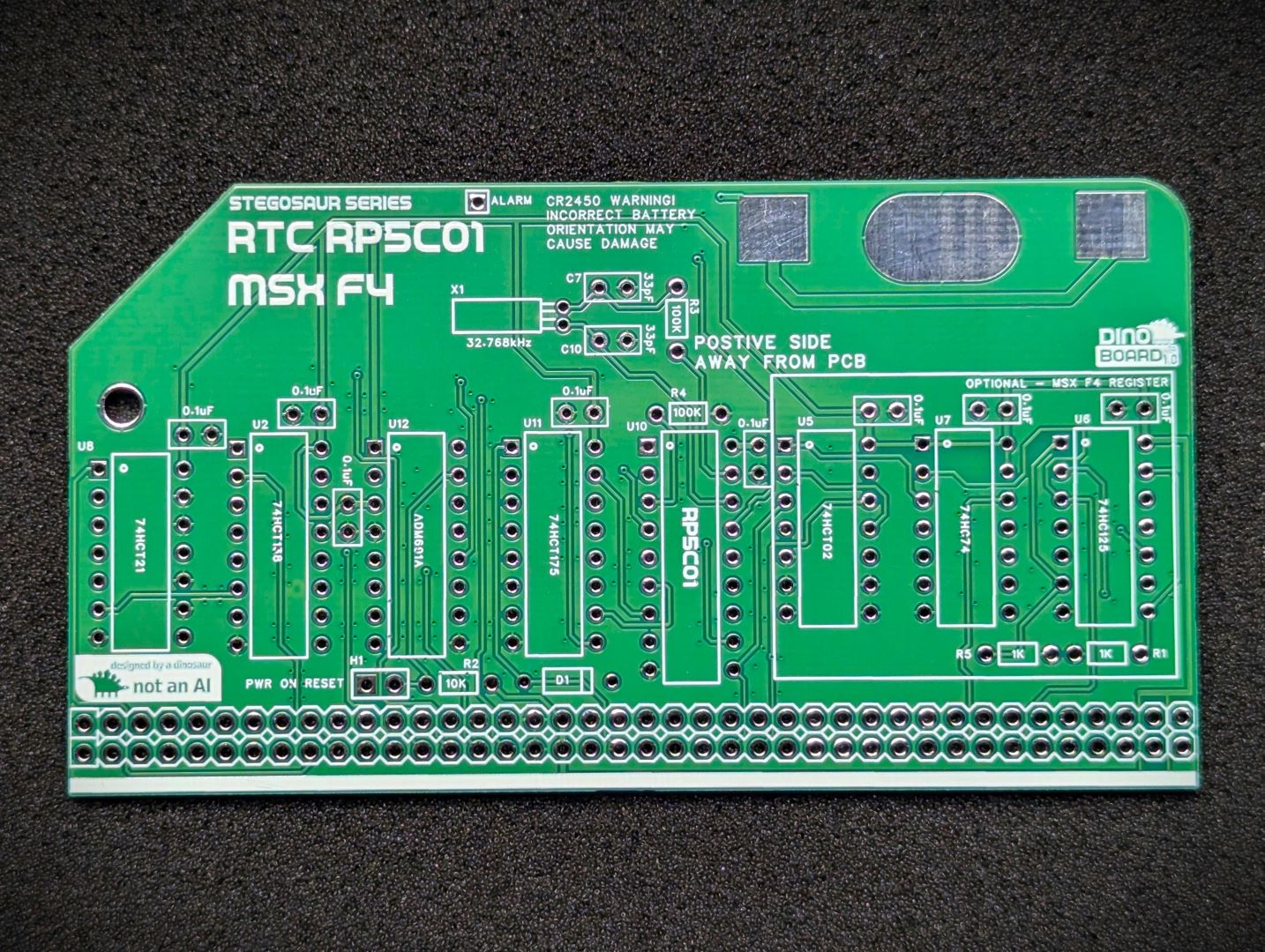 PCB Front |
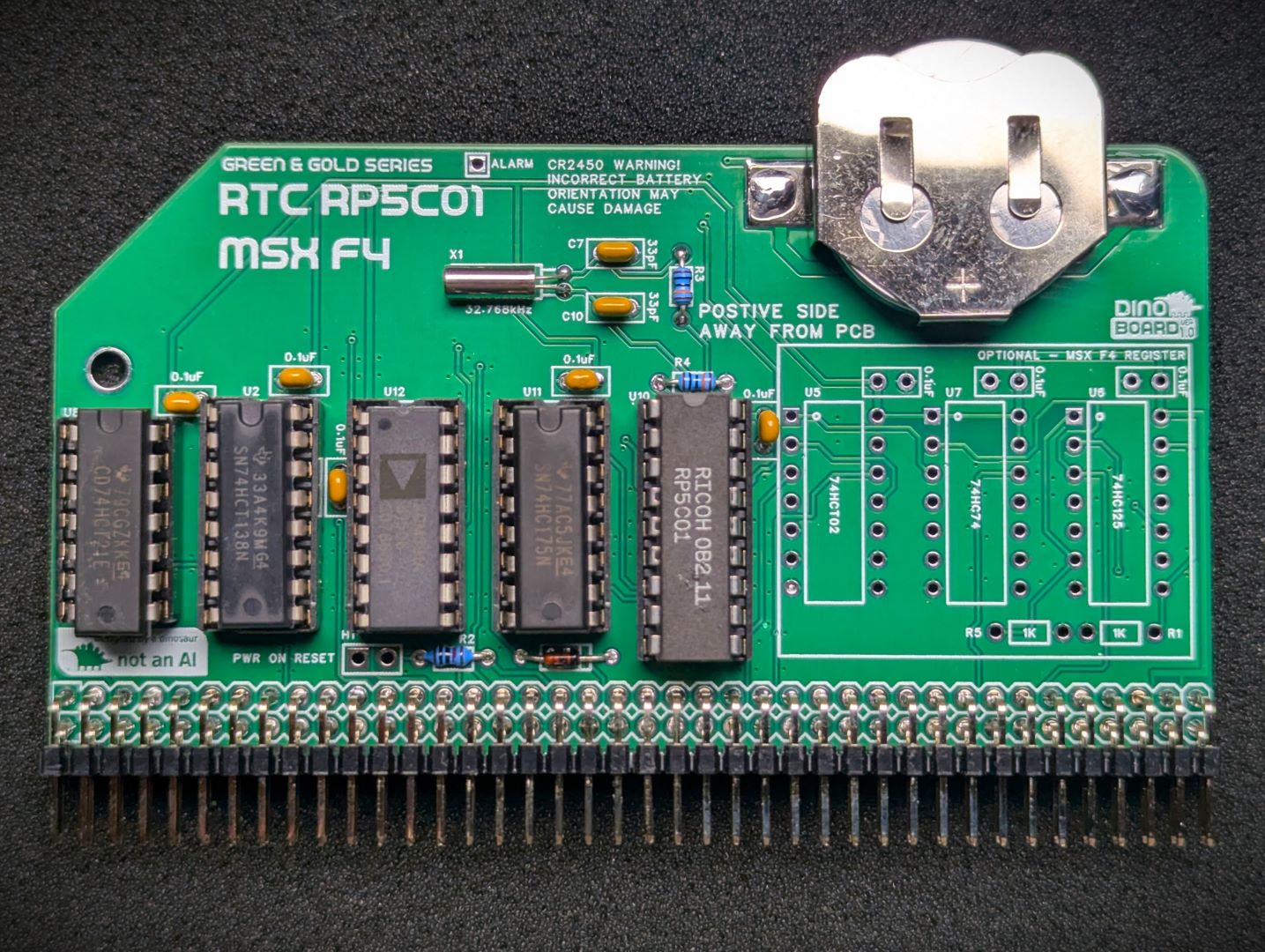
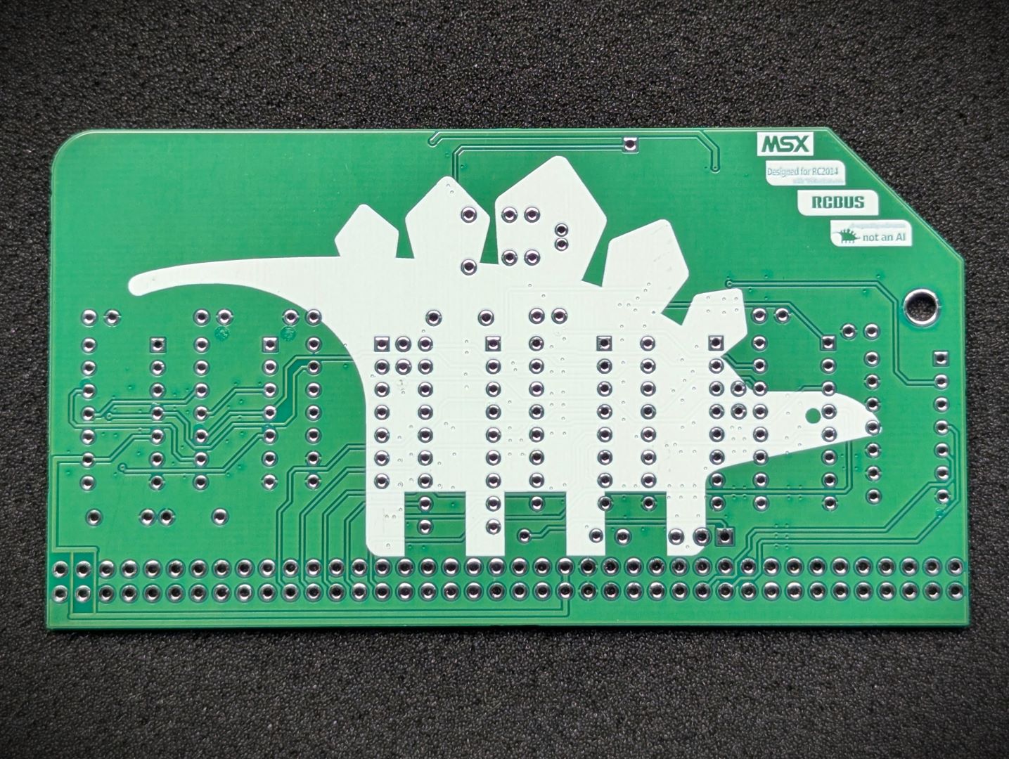 PCB Back |
* Self Source Reference are supplied as a guide only. Please double check, in case of typo or errors in listing.
| Count | Name | Self Sourcing* |
|---|---|---|
| 1 | CR2450 Battery Holder | |
| 5 | 0.1uF Ceramic Capacitors | Mouser: 594-K104K10X7RF53L2 DigiKey: BC5137-ND |
| 2 | 33pF | |
| 1 | 1N4148 | |
| 1 | Header 1x2 | |
| 1 | Shunt 1x2 | |
| 2 | 10K Ω (3.4mm) | |
| 1 | 100K Ω (3.4mm) | |
| 1 | 74HCT175 | |
| 1 | 74HCT138 | |
| 1 | 74HCT21 | |
| 1 | 32.768KHz | |
| 2 | Right Angle 2x20 Header | Mouser: 649-68020-140HLF DigiKey: 2057-PH2RA-40-UA-ND |
| 3 | 16 POS IC SOCKET | Mouser: 571-1-2199298-4 DigiKey: 2057-ICS-316-T-ND |
| 1 | 14 POS IC SOCKET | Mouser: 571-1-2199298-3 DigiKey: 2057-ICS-314-T-ND |
| 1 | 18 POS IC SOCKET | Mouser: 571-1-2199298-5 DigiKey: 2057-ICS-318-T-ND |
| Count | Name | Self Sourcing* |
|---|---|---|
| 1 | ADM691A | |
| 1 | RP5C01 |
| Count | Name | Self Sourcing* |
|---|---|---|
| 3 | 0.1uF Ceramic Capacitors | Mouser: 594-K104K10X7RF53L2 DigiKey: BC5137-ND |
| 2 | 1K Ω (3.4mm) | |
| 1 | 74HCT02 | |
| 1 | 74HC125 | |
| 1 | 74HC74 | |
| 3 | 14 POS IC SOCKET | Mouser: 571-1-2199298-3 DigiKey: 2057-ICS-314-T-ND |
The full kits includes everything you need (PCB, capacitors, IC sockets, connectors, and the ICs), with the retro chips optionally included.
The set of tested retro chips can be optionally included, or you can source your own.
The parts to enable the MSX specific F4 register feature can be optionally included.
A battery is not included. Requires a standard coin CR2450 battery.
This module can work in a standard RC2014/RCBus RomWBW bootable system, or a MSX configured bootable system.
The circuits power is managed by the ADM691 based supervisory circuit. This chip maintains power to the RP5C01 by switching between the battery and the main power.
The ADM691 chip has the ability to generate a reset signal, when main power is turned on. This can be mapped to the Z80’s reset line to ensure the CPU always has a clean reset at startup.
There is a jumper (H1) on the board to map this signal to the RESET line on the backplane. If you jumper this line, it will drive the RESET low on initial powering. This is an open drain connection - as such it does not hold the line high.
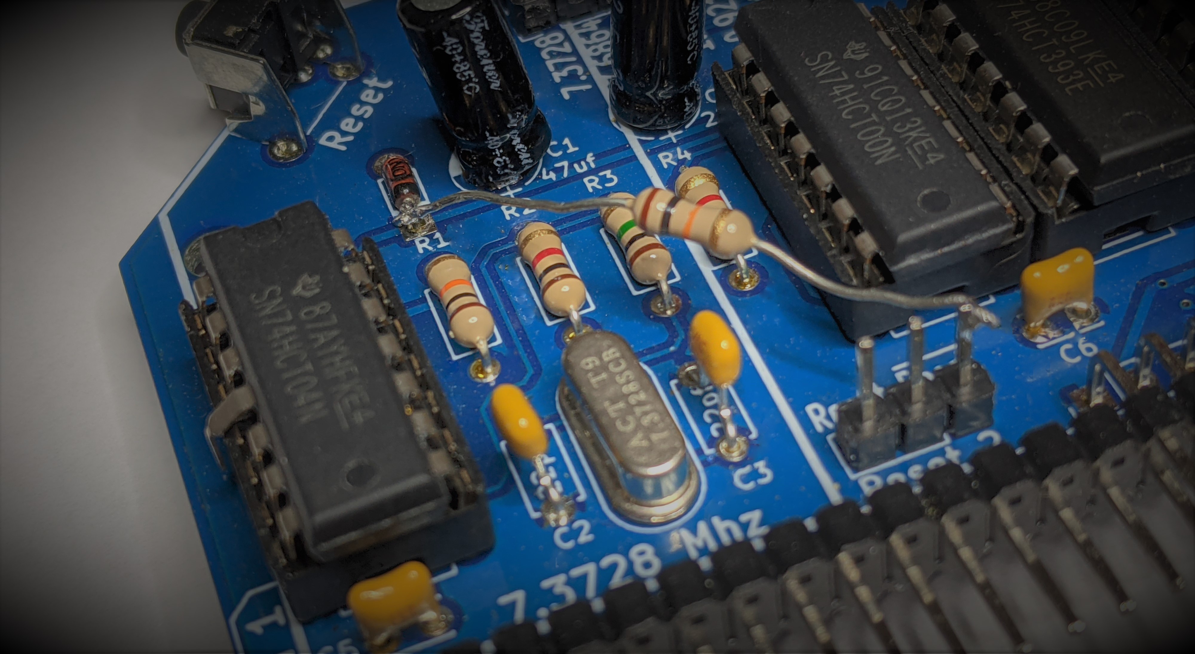
The RC2014 Dual Clock Module, also has a reset on power circuit. The Dual Clock Module’s circuit does have an issue - see Paul Williamson’s Must Be Art Blog Post for details and a specific modification.
For my specific setup, the Dual Clock’s Reset on Power circuit would not always reliably trigger a reset. And so I decided to disable it and use the Reset on Power function provided by the ADM691 chip.
My modification is simpler than that applied by Paul Williamson’s posting, as I just wanted to fully disable the circuit. (But i still needed the line to be held high with a pull up resistor)
My modification was to:
Disconnect the connection between the 74HCT04 gate output and the RESET line.
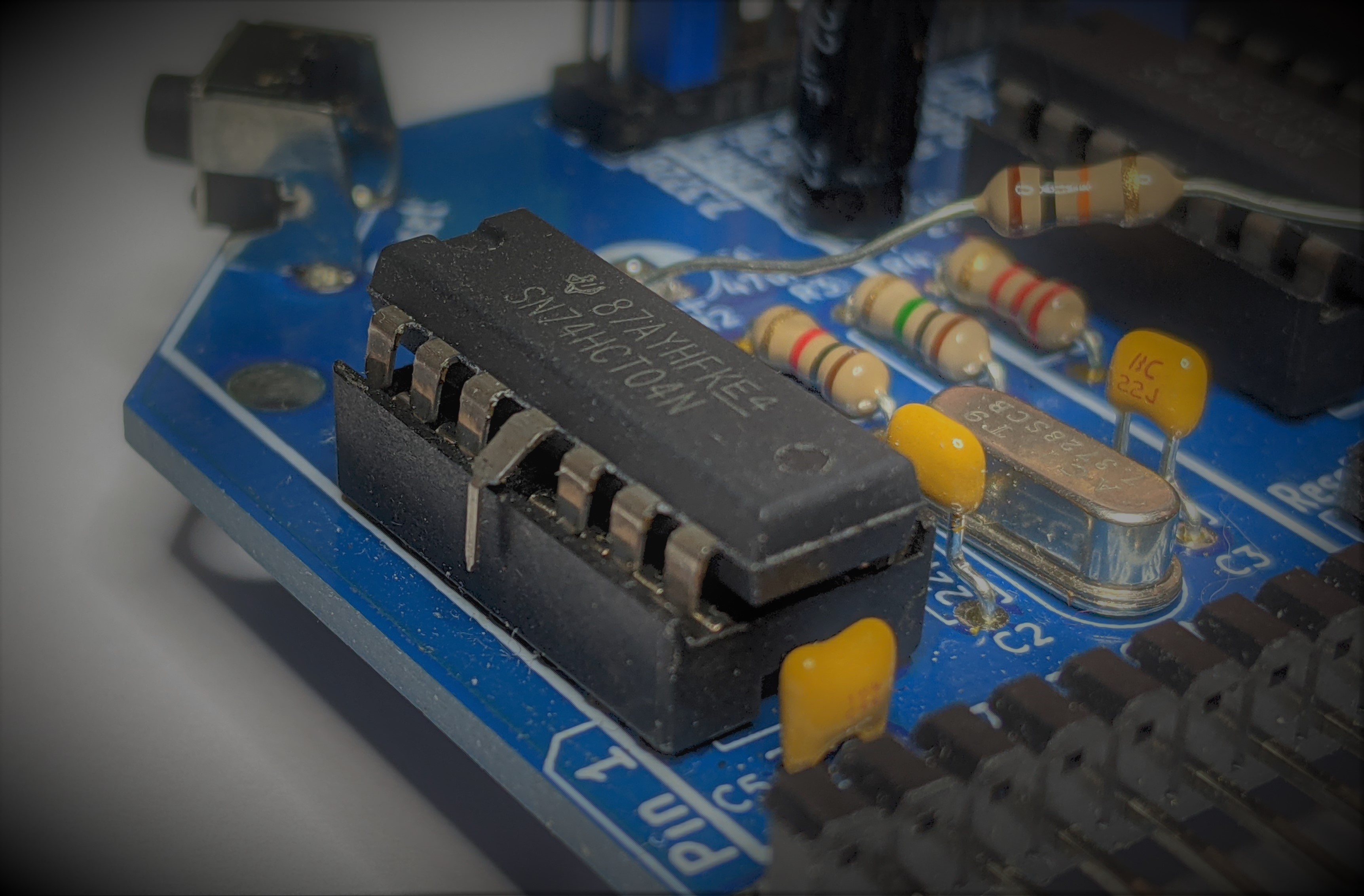
Apply a 10K resistor to the RESET line and VCC. I used the cathode point of D1 as shown:
You can access the chip directly thru the relevant ports, but under MSX, the ‘correct’ way is via the sub-rom bios calls:
REDCLK
Address  : #01F5
Function : Read clock-RAM
Input    : C  - clock-RAM address
                xxBBAAAA
                  ||++++-- address
                  ++------ Block-number
Output   : A  - Read value in lowest four bits
Registers: F

WRTCLK
Address  : #01F9
Function : Write clock-RAM
Input    : C  - clock-RAM address
                xxBBAAAA
                  ||++++-- address  :
                  ++------ Block-number
           A  - Value to write
Registers: F
For more information on how to use and program the chip, checkout the msx.org page.
The MSX2+ standard introduced the F4 Boot register. This is a register that, only when power is first applied, will reset itself. Thereafter only a software command will change the state of the register. For example, when the user reset the computer, the state of this register is not altered. This allows the software to know if the system had a cold or warm boot.
MSX2+ system roms utilised this capability, to skip ram checks and the logo/boot screen, during warm boots.
You can read the boot status, by reading the port at, you guessed it, $F4. The MSX bios will on a cold boot, reset BIT 7 of this register. The MSX bios has a couple of functions related to this register (RDRES, WRRES).
RDRES
Address  : #017A
Function : Read value of I/O port #F4
Input    : None
Output   : A = value read
Registers: AF

WRRES
Address  : #017D
Function : Write value to I/O port #F4
Input    : A = value to write
           When bit 7 is reset it shows the MSX 2+ startup screen on boot,
           and counts and initialises the RAM.
Output   : None
Registers: None
A driver for this chip has been submitted and accepted by Wayne Warthen and is now included in the main release.
Short this jumper to enable the power on reset feature.
Please see the Power On Reset Compatibility section above
| Port | Description |
|---|---|
| B4 | RP5C01 Register Selection |
| B5 | RP5C01 Data R/W |
| F4 | BIT 7 Cold/Warm Boot state |
| Description | Yellow MSX Version | Green Stegosaur Version |
|---|---|---|
| Calibration | on board trimmer capacitor | none |
| Battery | CR2032 | CR2450 |
| Diagnostic ‘Alarm/Timing’ Signal | exposed with pull up resistor | Exposed, but no pull up resistor |
| PCB Height | 8.0 cm | 5.5 cm |
| Colour | Yellow | Green |
Generally, you want to solder items from lowest height to largest height. Review the components you need to solder, and note their progressive heights.
* Note the right angle headers are position correctly and lay flush and at right angle to the main PCB.
Please note the following specific points regarding this module:
Before soldering the (CR2450) battery holder, you may want to place a small amount of solder on its ground pad. This will ensure a good contact when you insert a battery.
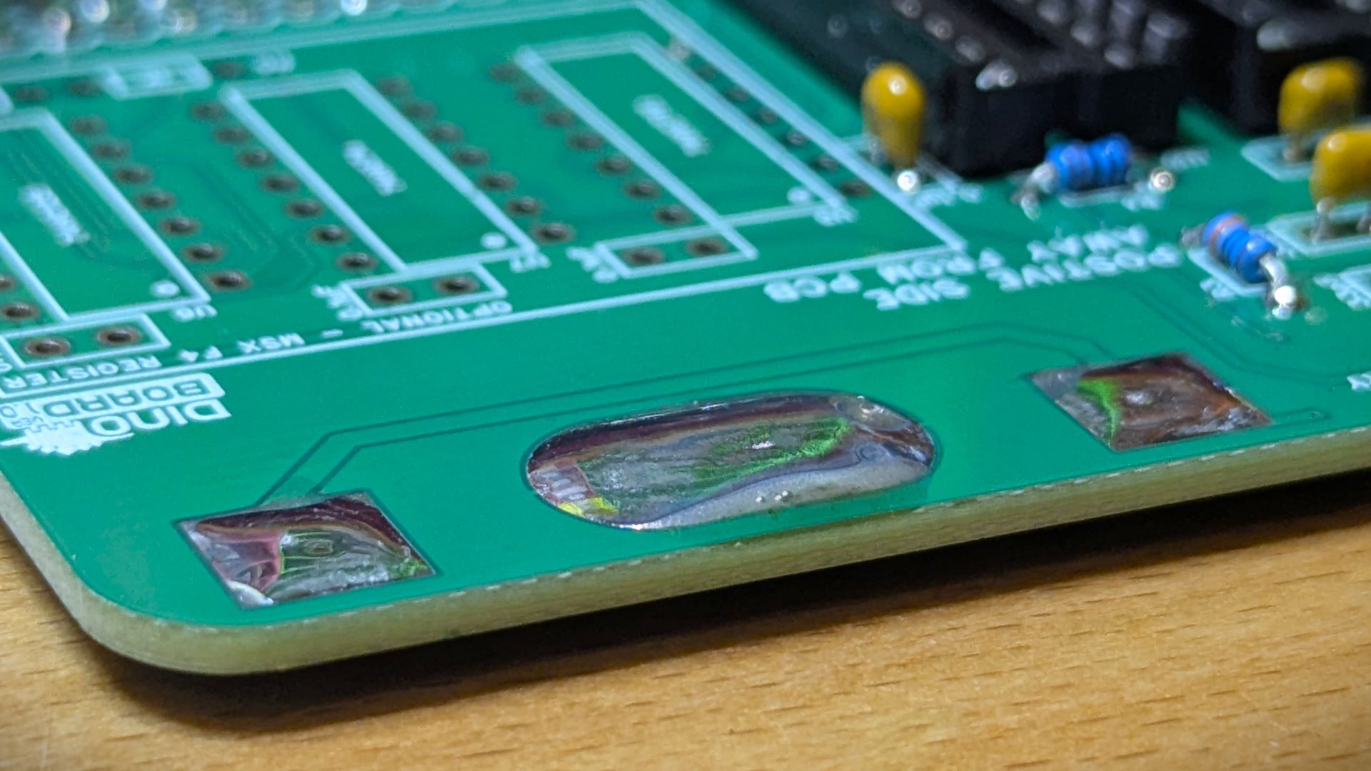
Also you may find it easier to apply a small amount of solder to the main positive pads. Secure the battery holder down with some tweezer, then apply heat to seat the holder flush to the PCB.
Please note that this is a kit, produced by a non-expert (me) for hackers, DIYers’ and retro lovers, to tinker with. Please exercise caution and follow good safety practices. You will be working with sharp knives, a hot soldering iron, and small metal components. Be mindful of the risks involved in the build process. I will do my best to answer any questions you may have.
This kit is provided as-is, with no guarantees or warranties. By assembling and using this kit, you acknowledge that you do so at your own risk.
 Store
Store