Code: DB301
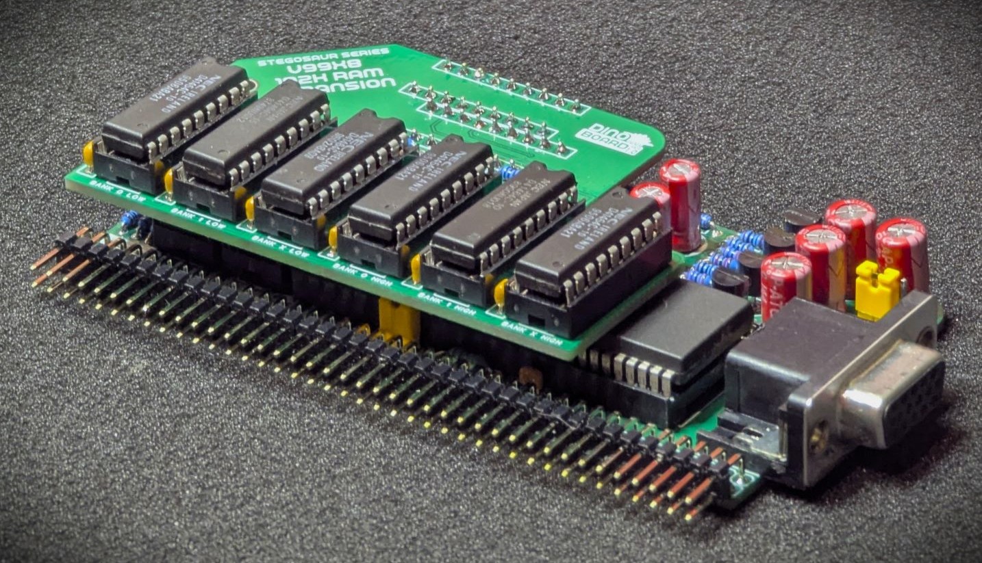
Memory Expansion: DB302
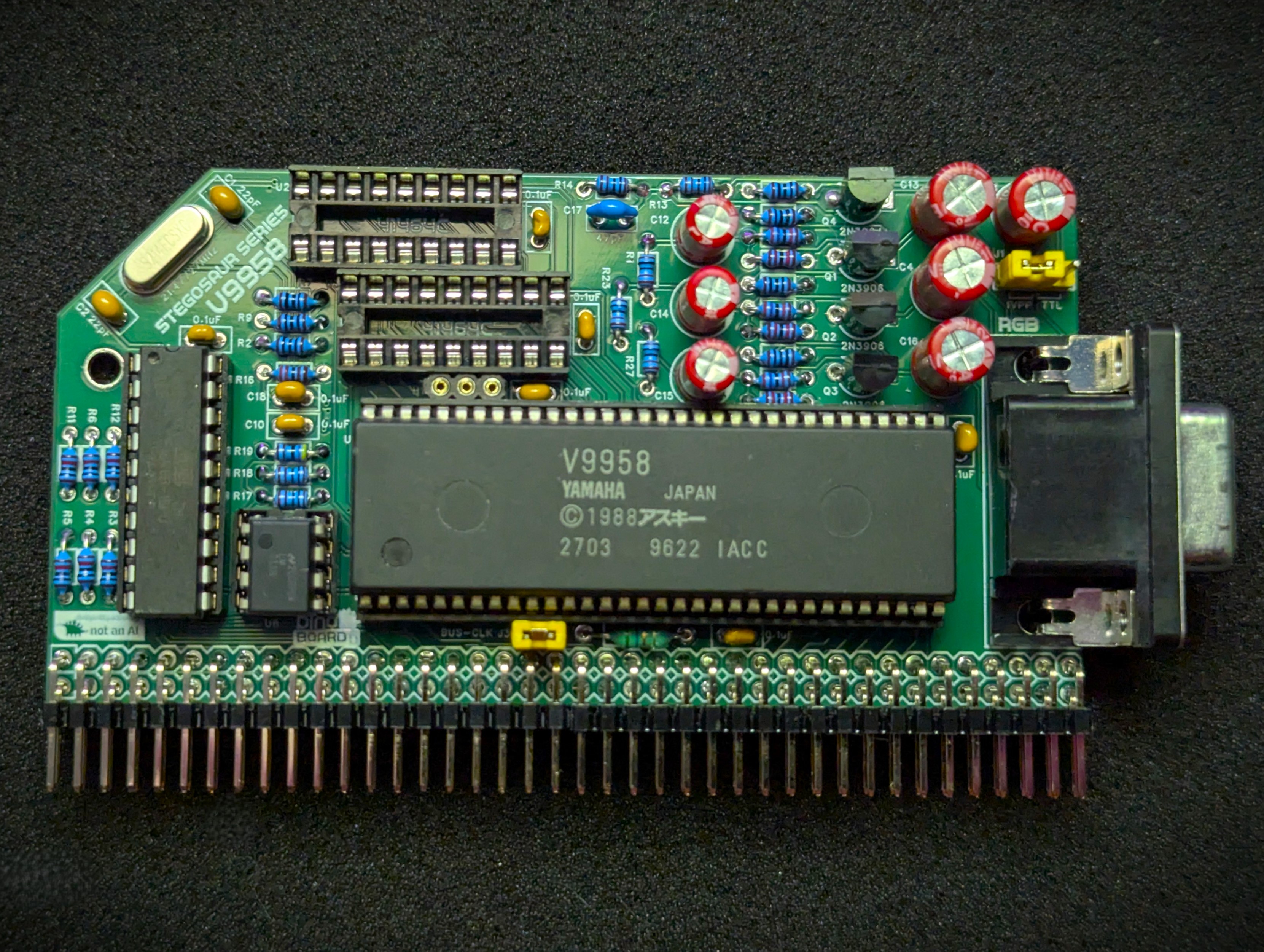
A complete kit to give your RC2014/RCBus platform, the advanced graphic capabilities of the mid to late 80s. It based around the V9958 Video Display Processor (VDP) which powered the MSX2/MSX2+ line of 8 bit Z80 computers.
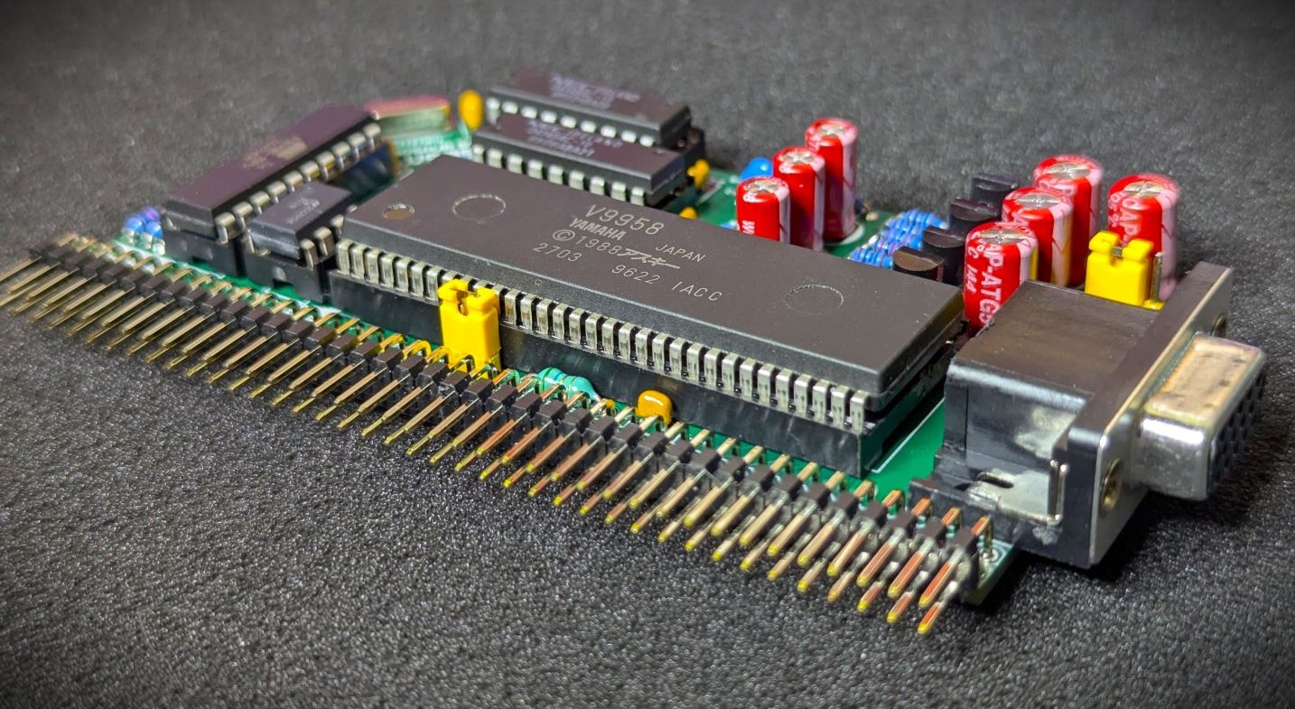
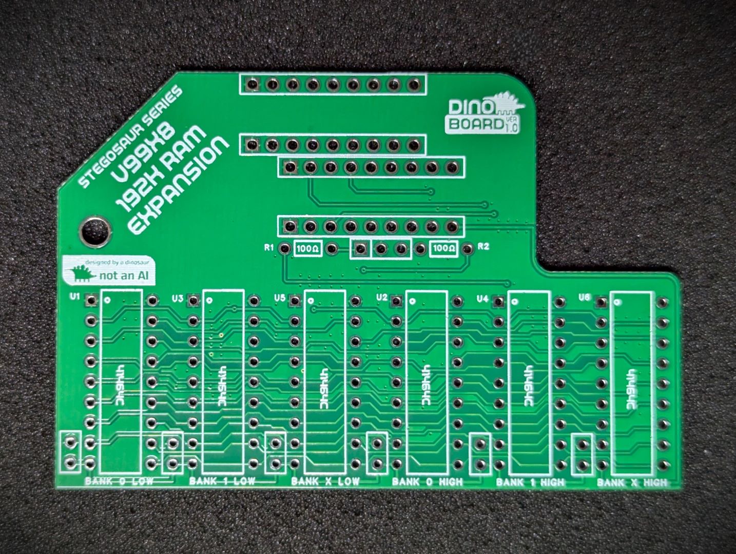
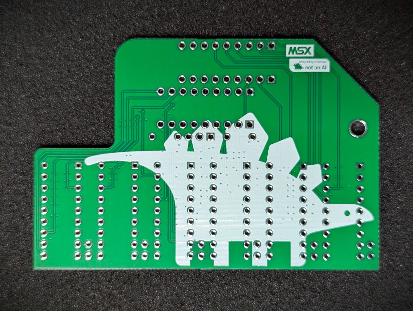
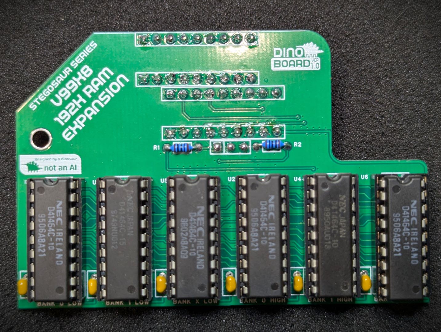
The main PCB supports the installation of 64K of VRAM, sufficient for all screen modes of the processor. With the use of the optional expansion board, the VRAM can be extended to the full 192K of VRAM that the V9958 is able to address.
This V9958 chip, was produced by Yamaha in the late 80s and was an update to the the V9938 chip, which was itself, a successor to TI’s TMS9918. The V9938/V9958 addressed many of the shortcomings of the original TMS9918.
The V9938 and V9958 are very similar in capability. See the relevant datasheets below to get some details of the differences.
 |
 |
 |
 |
 |
 |
 |
 |
* Self Source Reference are supplied as a guide only. Please double check, in case of typo or errors in listing.
| Count | Name | Self Sourcing* |
|---|---|---|
| 2 | 22pF Ceramic Capacitor | |
| 1 | 47pF Ceramic Capacitor | |
| 8 | 0.1uF Ceramic Capacitors | Mouser: 594-K104K10X7RF53L2 DigiKey: BC5137-ND |
| 3 | 10uF | |
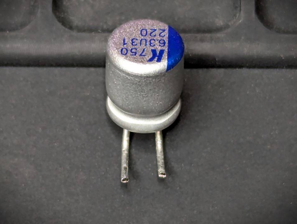
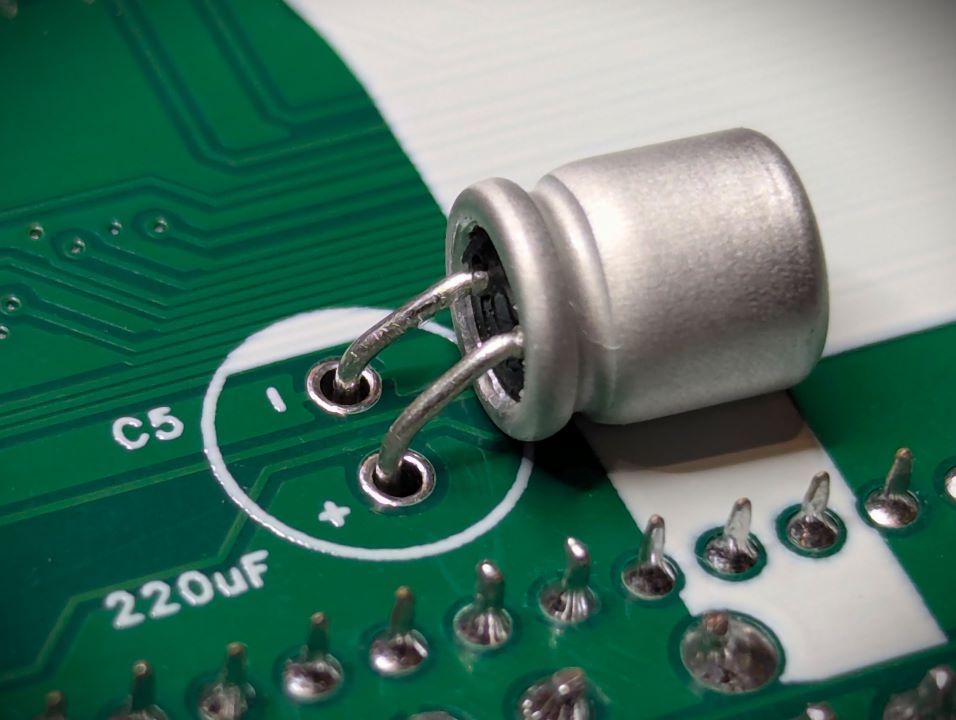
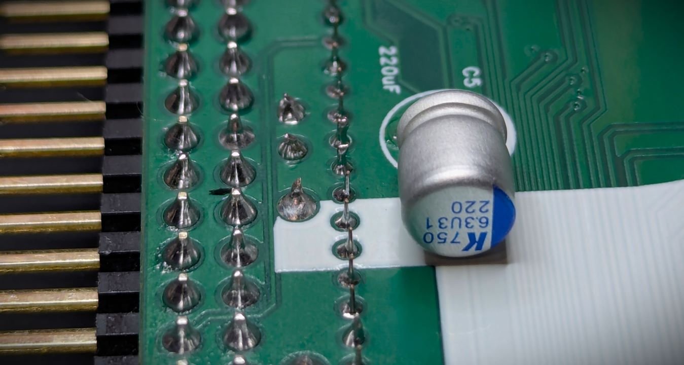
| 1 | 220uF (LOW ESR) | |
| 4 | 220uF | |
| 1 | Round Female Pin Header 1x40 | |
| 1 | HEADERS 1x3 | |
| 1 | HEADERS 1x2 | |
| 2 | Shunt 1x2 | |
| 1 | 5.6uH Inductor | Mouser: 871-B78108S1562K |
| 1 | 15-PIN DSUB | Mouser: 649-ICD15S13E4GV00LF DigiKey: 609-5180-ND |
| 3 | 2N3906 | Mouser: 637-2N3906 |
| 1 | 2N3904 | Mouser: 637-2N3904 |
| 6 | 10k Ω (3.4mm) | Mouser: 603-MFR-12FTF52-10K |
| 3 | 12k Ω (3.4mm) | Mouser: 603-MFR-12FTF52-12K |
| 3 | 27k Ω (3.4mm) | Mouser: 603-MFR-12FTF52-27K |
| 1 | 4k7 Ω (3.4mm) | |
| 1 | 2k2 Ω (3.4mm) | Mouser: 603-MFR-12FTF52-2K2 |
| 7 | 1k Ω (3.4mm) | DigiKey: 13-MFR25SFRF52-4K7CT-ND |
| 1 | 470 Ω (3.4mm) | Mouser: 603-MFR25SFTF52-470R |
| 7 | 100 Ω (3.4mm) | Mouser: 603-MFR-12FTF52-100R |
| 1 | LM311N | Mouser: 926-LM311N/NOPB DigiKey: LM311NNS/NOPB-ND |
| 1 | ATF16V8B-15PU | Mouser: 556-AF16V8B15PU DigiKey: ATF16V8B-15PU-ND |
| 1 | 21.47727MHz | Mouser: 520-HCU2147-SX |
| 2 | Right Angle 2x20 Header | Mouser: 649-68020-140HLF DigiKey: 2057-PH2RA-40-UA-ND |
| 1 | 8 POS IC SOCKET | Mouser: 649-DILB8P223TLF DigiKey: AE9986-ND |
| 2 | 18 POS IC SOCKET | Mouser: 571-1-2199298-5 DigiKey: 2057-ICS-318-T-ND |
| 1 | 20 POS IC SOCKET | Mouser: 571-1-2199298-6 DigiKey: 2057-ICS-320-T-ND |
| 1 | 64 POS IC SOCKET | DigiKey: 1212-1068-ND |
| Count | Name | Self Sourcing* |
|---|---|---|
| 1 | V9958 VDP | |
| 2 | 41464C RAM |
| Count | Name | Self Sourcing* |
|---|---|---|
| 6 | 0.1uF Ceramic Capacitors | Mouser: 594-K104K10X7RF53L2 DigiKey: BC5137-ND |
| 2 | 100 Ω (3.4mm) | Mouser: 603-MFR-12FTF52-100R |
| 1 | Round Hole Pin Header 1x40 | |
| 6 | 41464C RAM | |
| 6 | 18 POS IC SOCKET | Mouser: 571-1-2199298-5 DigiKey: 2057-ICS-318-T-ND |
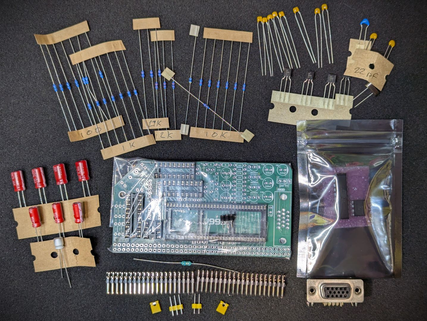
The full kits includes everything you need (PCB, capacitors, IC sockets, connectors, and the ICs), with the retro chips optionally included.
The tested V9958 and RAM chips can be optionally supplied, or you can source your own.
The optional VRAM Expansion kit is also supplied with main components, with tested RAM chips optionally included.
This module can work in a standard RC2014/RCBus RomWBW bootable system, or a MSX configured bootable system.
You will need a compatible display. See next section
You will want to think about how you plan to connect this board to your chosen monitor. The video signals produced by 80’s hardware is not trivial to connect to modern LCD monitors. For such monitors you will need a converter to upscale the output. Although VGA Monitors can accept a RGB signal, they are unlikely to support the lower frequency of 15Khz produced by this module.
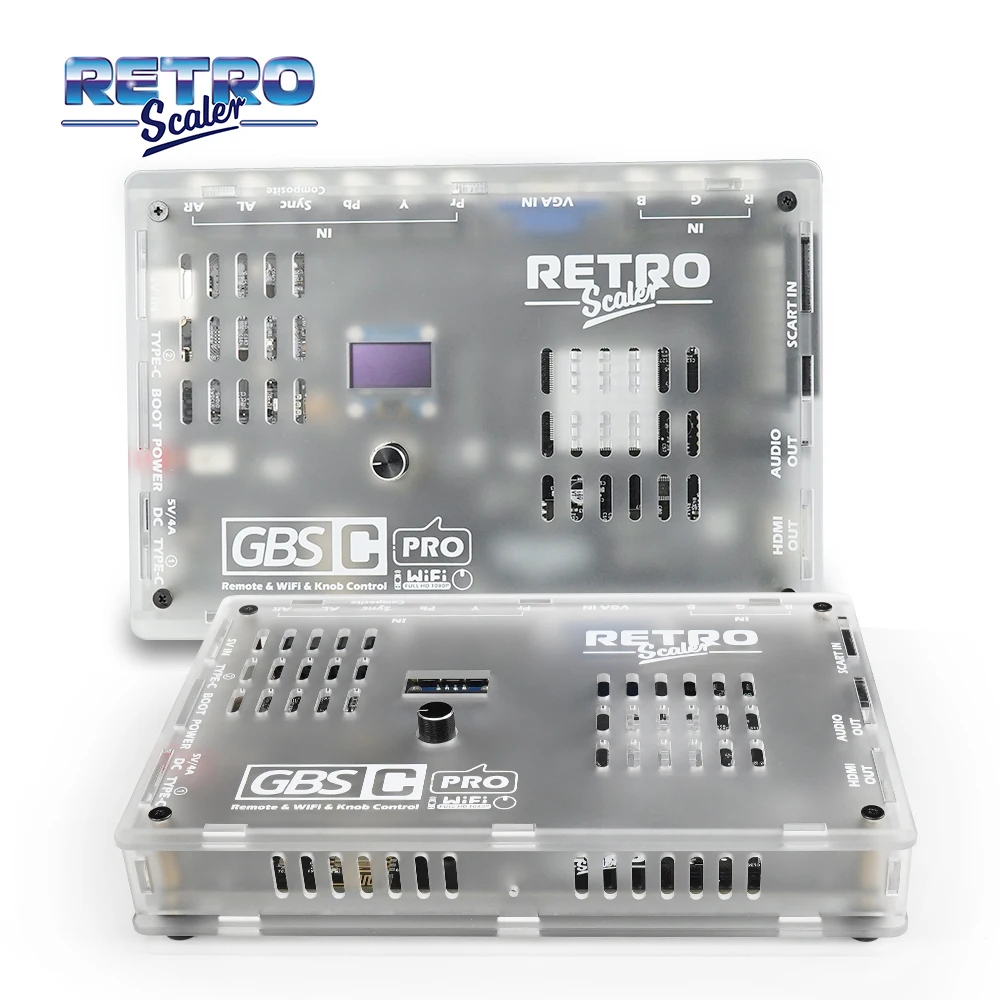
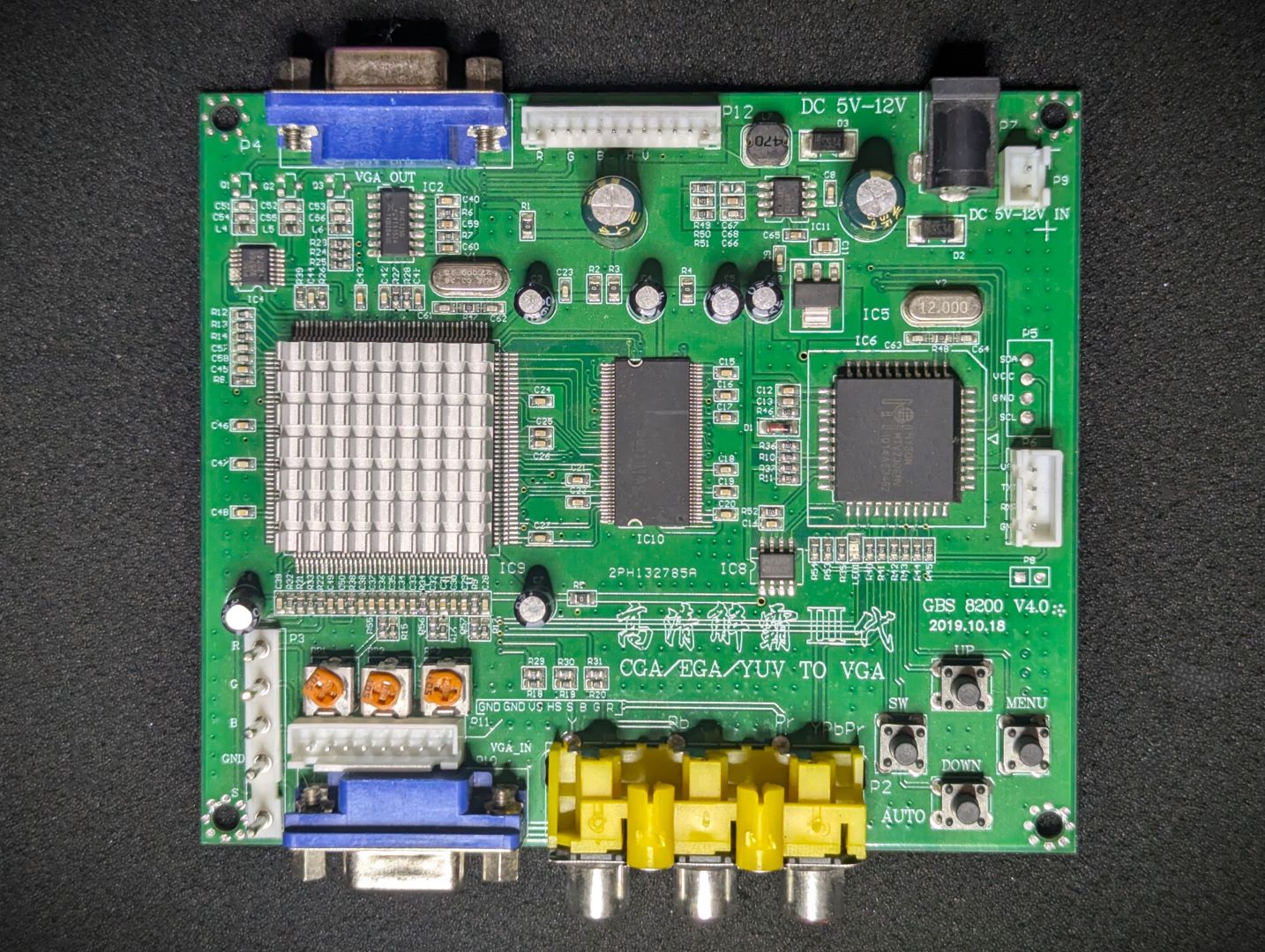
The RGBs module provides connection via the 15-pin DSUB/VGA connector. This output is well suited to connect via a VGA cable to a compatible HDMI/VGA up-converter that accepts a RGBs signal over the 15pin connection, such as the GBS-8200, HD-VC9900 or RetroScaler GBSC PRO converters. For more information on the DSUB RGB/VGA see RetroRGB’s VGA article
The RetroRGB upscalers article has a good description for some of the converter options.
Items such as retroTink and OSSC are very high quality converters - but also have a decent price tag.
I found the low cost arcade converters such as the GBS-8200 and HD-VC9900 converters produce ok results, but recent iterations of these products have downgraded quality quite a bit. I am unsure if these products have a consistent quality of operation and reliability when sourced from the various market places. I personally have had some units arrive that do not work as well (or at all) as other units.
The GBS-8200 can also be easily modified to produce more customisable and higher quality output, although this is a modification I have done done or tested personally. Again, RetroRGB has it all explained at GBS Control
My current recommendation, other than the high end converters such as retroTink and OSSC, is the RetroScaler GBSC PRO for HDMI conversion. The project is hosted on github here https://github.com/RetroScaler/gbsc-pro - which includes a link to their store to purchase a full unit. This product is a little more pricy than the stock GBS-8200, but you will unlikely have any conversion issues. I have tested with this unit, and found it produces excellent results.
| Pin | Signal |
|---|---|
| 1 | Red |
| 2 | Green |
| 3 | Blue |
| 4 | NC |
| 5-8, 10-11 | GND |
| 9, 12 | NC |
| 13 | CSync |
| 14,15 | NC |
My current recommended converter is the RetroScaler GBSC PRO . I have tested this unit and have found it produces excellent output to my HDMI 4:3 monitor.
I have also tested this kit with success, using the low cost GBS-8200 and HD-VC9900 upscalers. These have mostly produced solid stable images for the respective VGA and HDMI output. They seem very tolerant of CSYNC voltage signal levels.
But I can no longer recommend the use of the GBS-8200 or the HD-VC9900 upscalers. I have found that the quality of the units can vary, depending on specific iteration and some units I have recently purchased do not convert at all.
If you do wish to try the GBS-8200, I do recommend the V4.x version and not the V5.x version. The V5.x produces a poorer quality output. You can identify the V4 revisions by the colour of the menu control buttons. Black for V4 and Yellow for V5.
 GBS8200 - V4 Recommended* |
 GBS8200 - V5 Not Recommended |
* Caveat with the GBS-8200 recommendation is that I have found some units fail to convert. Its possible there is a firmware variation at play. I suspect, but have not confirmed, that the GBS-Control modification may resolve the issue.
Other upscalers, such as the OSSC and retroTink probably work very well, but I am unable to verify and confirm. Your milage may very. Adapter cables may need to be constructed.
I have not tested the unit on a real RGB CRT monitor.
I have been advised by some builders of the Yellow version of this kit (which has an identical RGB output stage as this module), that they have successfully tested with a real CRT, the OSSC and retrotink devices.
For a base ROMWBW build you can find compatible demo apps in the apps-rc2014 directory on the github project site. They can be run under CP/M on a RC2014 system. The prebuilt binaries can be found in the bin directory.
For a MSX-DOS system, binaries for various apps and demos can be found in the github releases
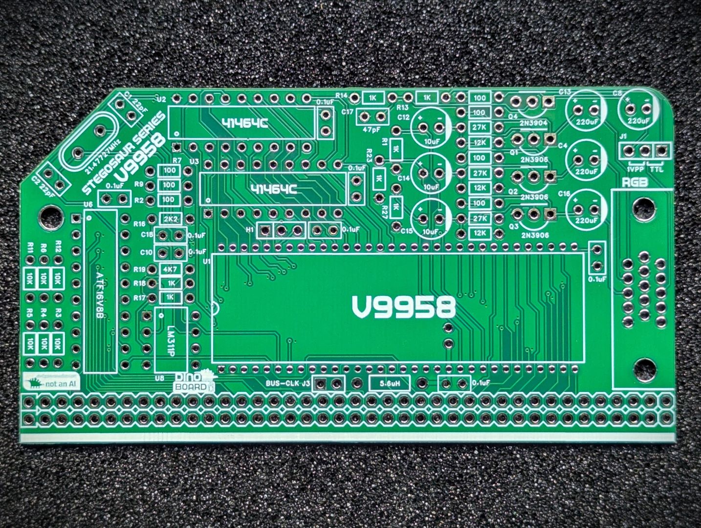
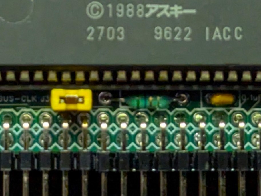
This jumper allows for the selection of the voltage level of the CSYNC output. (1VPP or a 5V TTL). For original CRT and old compatible 15Khz monitors, its recommended to set this to 1VPP (short the 2 left pins).
Most upscalers are likely to tolerate a 5V TTL level signal, but supplying 5V signal to a system that expects 1VPP may cause damage to the device. So it is only recommended to set this to the 5V TTL level when the connecting device states it accepts or needs such a signal type.
Shorting this jumper, will transmit the clock signal generated by the VDP (3.579545Mhz) to the RC2014/RCBus’s CLK1 lane. This clock signal can then be used to drive your Z80 CPU. Do not short this if you have another clock generator on your platform. For best MSX compatibility, it is recommended to use this clock signal (1/6 of the main V99x8 crystal frequency), and remove any other CLK1 generators.
The board uses the standard IO addresses for MSX systems.
The first 2 ports are identical as per the TMS9918 chip. The V9938/58 have additional ports to access higher functions.
| Port | Description |
|---|---|
| $98 (r/w) | VRAM data |
| $99 (w) | VDP register selection |
| $99 (r) | Status register |
| $9A | Palette access |
| $9B | Indirect register access |
Have a look at the sample apps included in this repo apps-rc2014.
For specific details on programming the chip, I recommend:
| Description | Yellow MSX Version | Green Stegosaur Version |
|---|---|---|
| Max VRAM on main board | 128K | 64K |
| VRAM Expandable? | No | Yes (up to 192K) |
| V9958 and V9958 Support | Single PCB can support both VDP types | Different PCB needed for each VDP type |
| V9958 WAIT signal supported | Yes | No |
| RGB Video output design | unchanged | unchanged* |
| Optional 5V out via RGB Connector | Yes | No |
| PCB Height | 8.0 cm | 5.5 cm |
| Colour | Yellow | Green |
* The Green Stegosaur RGB kit utilizes separate PCB designs for the V9938 and V9958 VDPs. This allows the V9958’s PCB, to refine the layout and tracing of the power delivery components for the V9958’s DAC; minimising, as much as possible, potential EM interference appearing on your display.
Generally, you want to solder items from lowest height to largest height. Review the components you need to solder, and note their progressive heights.
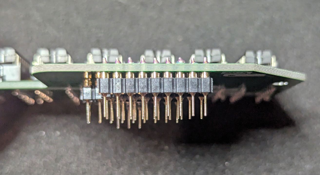
* Note the right angle headers are position correctly and lay flush and at right angle to the main PCB.
Please note the following specific points regarding this module:
Due to the finer pitch pins of the V9958, the soldering of this board requires a little more finesse than the typical RC2014 through-hole based boards. If you have built a few boards already, then you should be fine. It’s recommended that a finer pitch soldering tip be used as it can be easy to accidentally bridge some of the pins.
Extra care needed when inserting the V9958 into its socket - there are lots of pins, take your time to avoid bending pins.
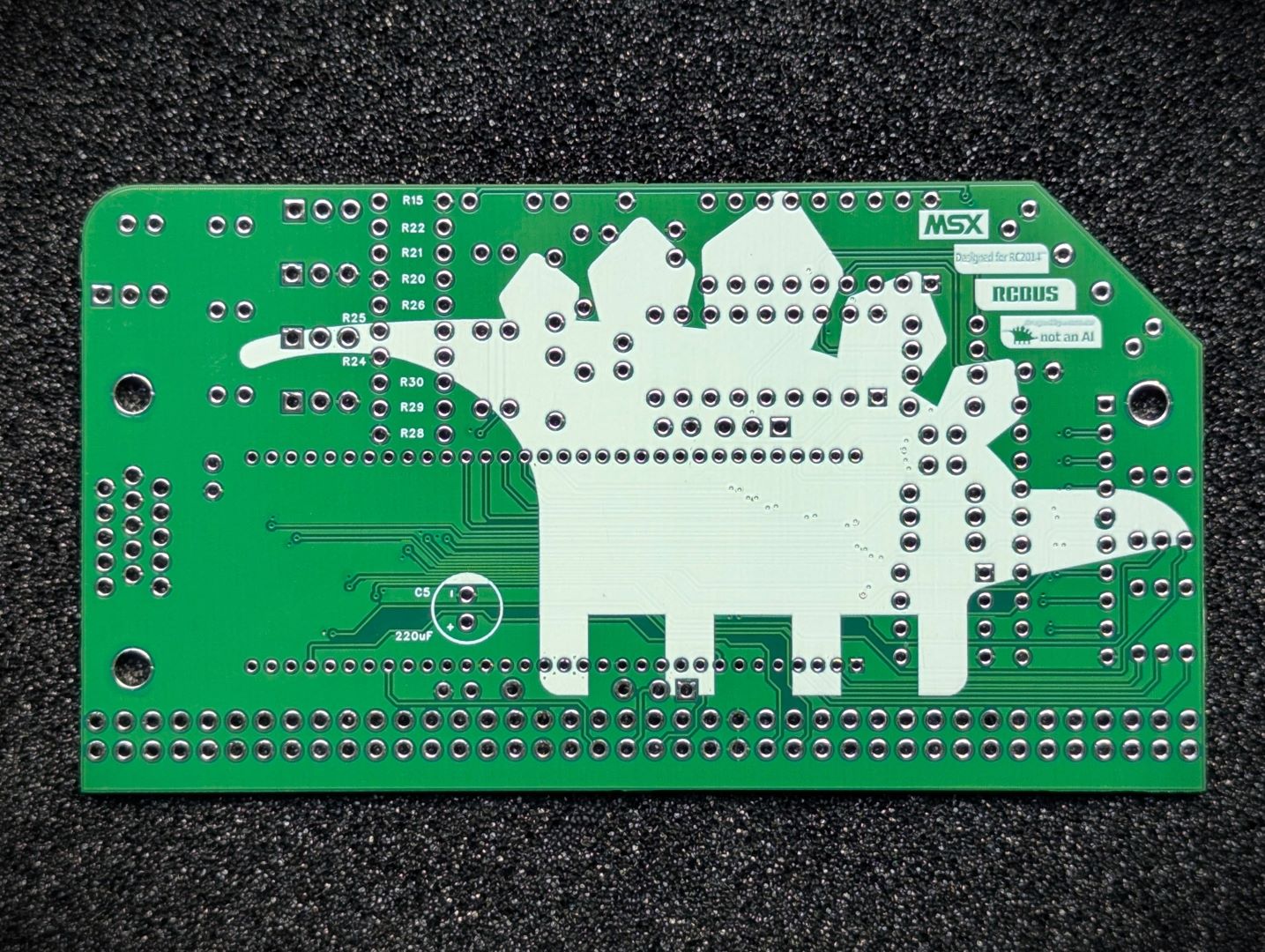
There is a 220uF capacitor that, due to space constraints, needs to be mounted on the back of the PCB. You can choose to solder this first and applying solder on the front of the PCB. But my personal recommendation is to solder it last. After all other components have been soldered, you can place the capacitor over on its side, as shown below, clipping the wires as required before inserting, and then soldering on the underside of PCB.

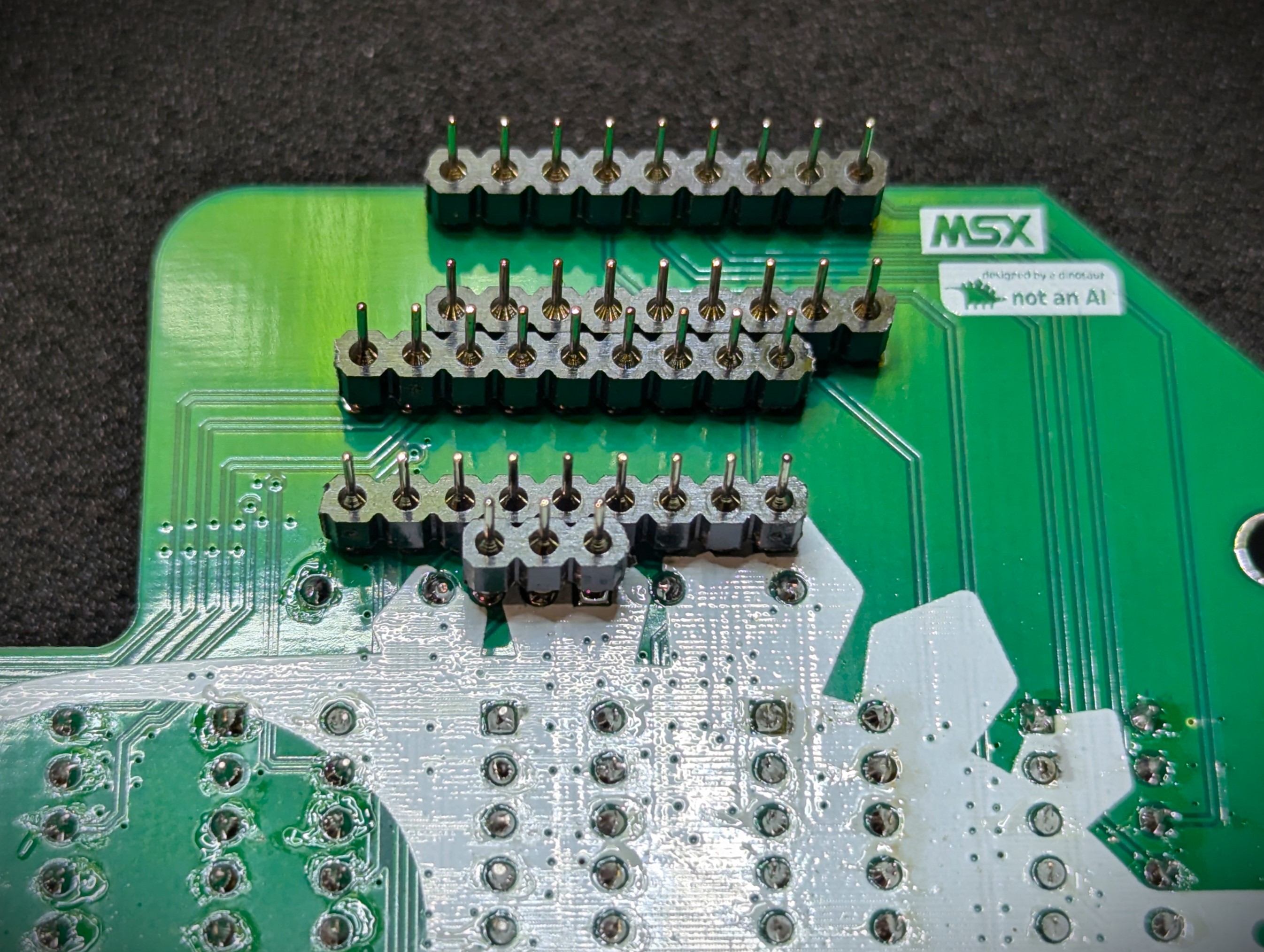
Ensure the 1 x 3 Round Machine Header (low profile) is mounted straight and flush, to ensure a good fit for the optional memory expansion board.

Pay close attention to the position of Jumper J3 1 x 2 header, the 5.6uH inductor and 0.1uF capacitor, as they have a minimal fit between the 64pin IC socket and mounting right angler header.
The bottom of the VRAM exapnsion RAM module, once soldered, will make contact with the V99x8 VDP plastic cover. The PCB is designed to be installed at a slight angle. To ensure a good fit perform the assembly in the following process:
Note the orientation of how the round headers need to be soldered to the expansion module.
Please note that this is a kit, produced by a non-expert (me) for hackers, DIYers’ and retro lovers, to tinker with. Please exercise caution and follow good safety practices. You will be working with sharp knives, a hot soldering iron, and small metal components. Be mindful of the risks involved in the build process. I will do my best to answer any questions you may have.
This kit is provided as-is, with no guarantees or warranties. By assembling and using this kit, you acknowledge that you do so at your own risk.
 Store
Store