Code: DB213
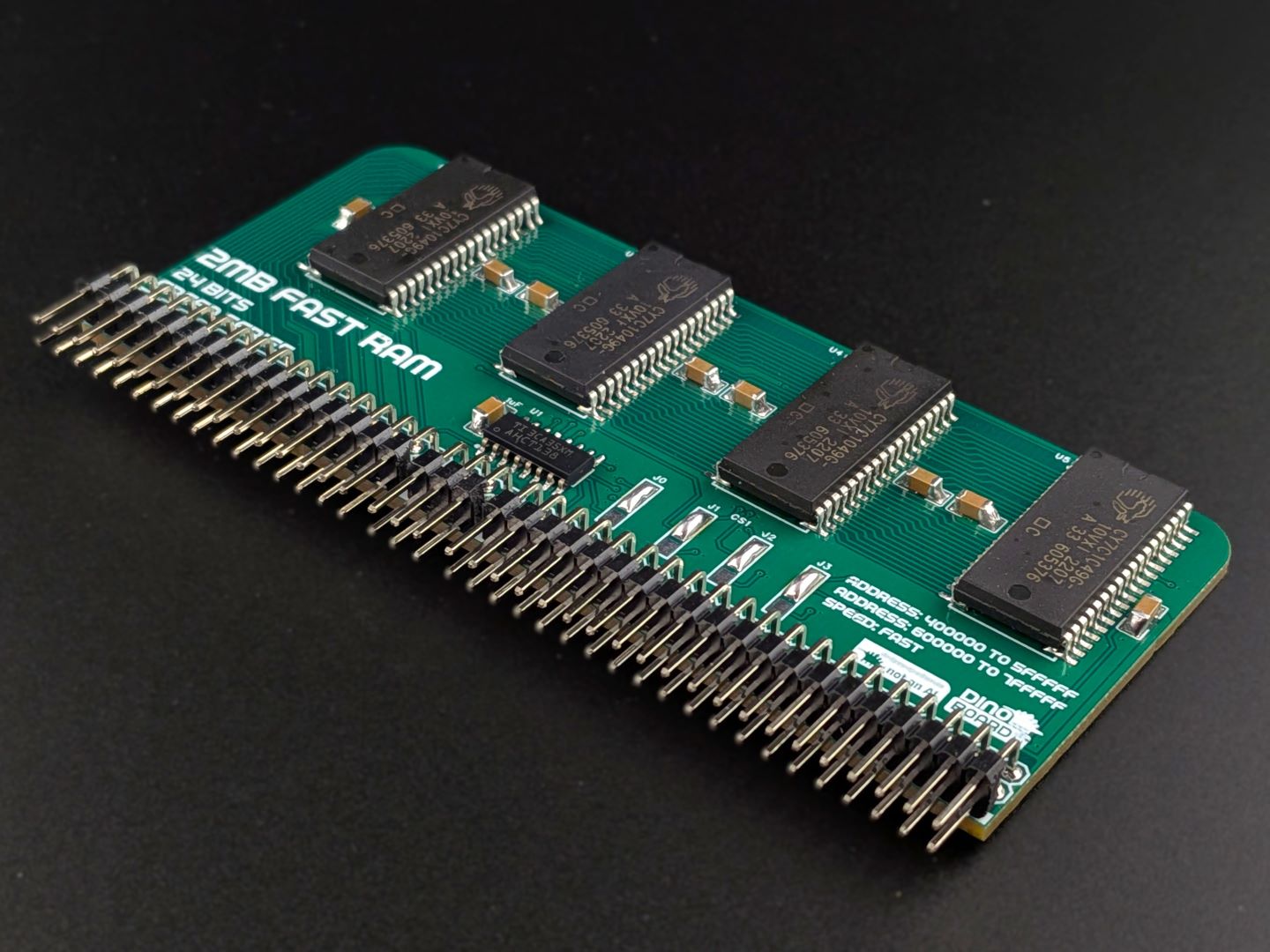
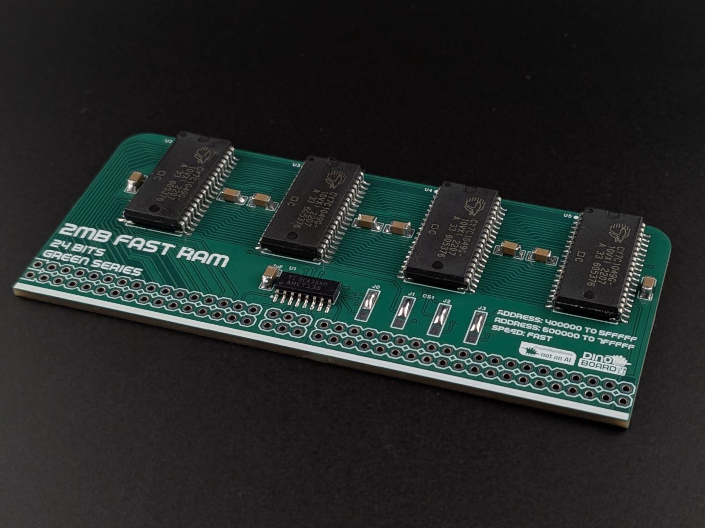
An alternative to the RCBus 2MB linear memory module, this module uses a specially designed interface to allow for high speed memory operation. Break the 64K barrier with this high speed memory module designed for the ozRaptor module
The ozRaptor module supports up to two of these modules, to allow for up to 4MB of linear direct access 0 wait state memory.
A key feature of the eZ80 CPU is its 24bit addressing capability allowing programs to be written that can utilise up to 16MB of memory natively. No paging or banking hardware needed. No need for applications to be developed that limit themselves to 64K or complex paging mechanisms.
Unlike standard Z80 memory modules that only works with a 16-bit address, the Fast 2MB Linear RAM module is specifically designed to take full advantage of the eZ80’s 24-bit address space. It provides a continuous 2MB block of memory that can be directly accessed by the eZ80, making it possible to build or port larger programs.
 |
 |
 |
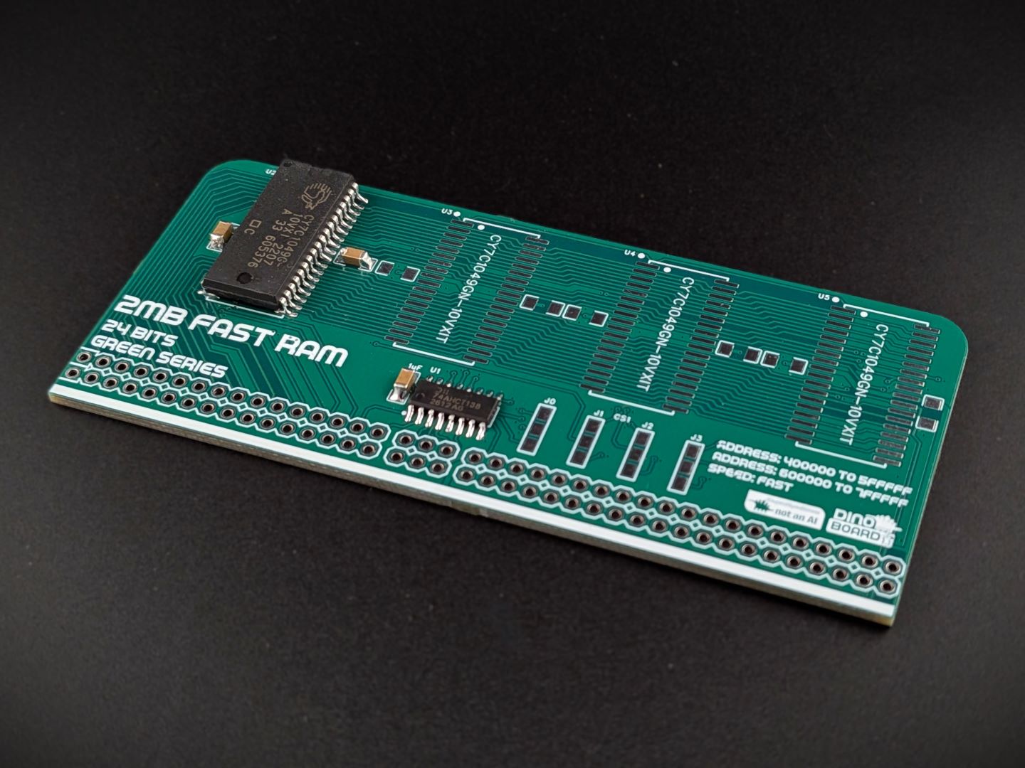 |
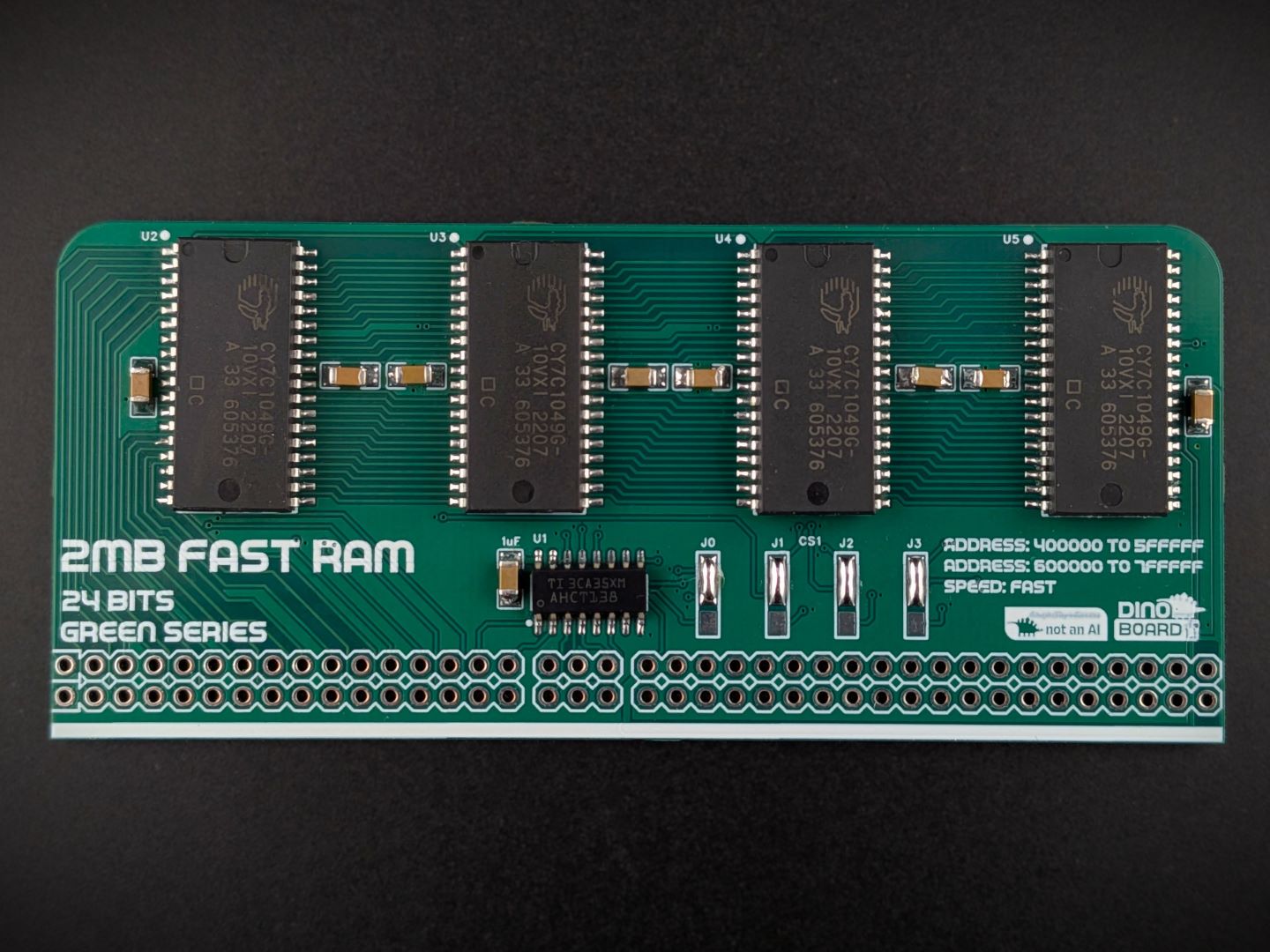 |
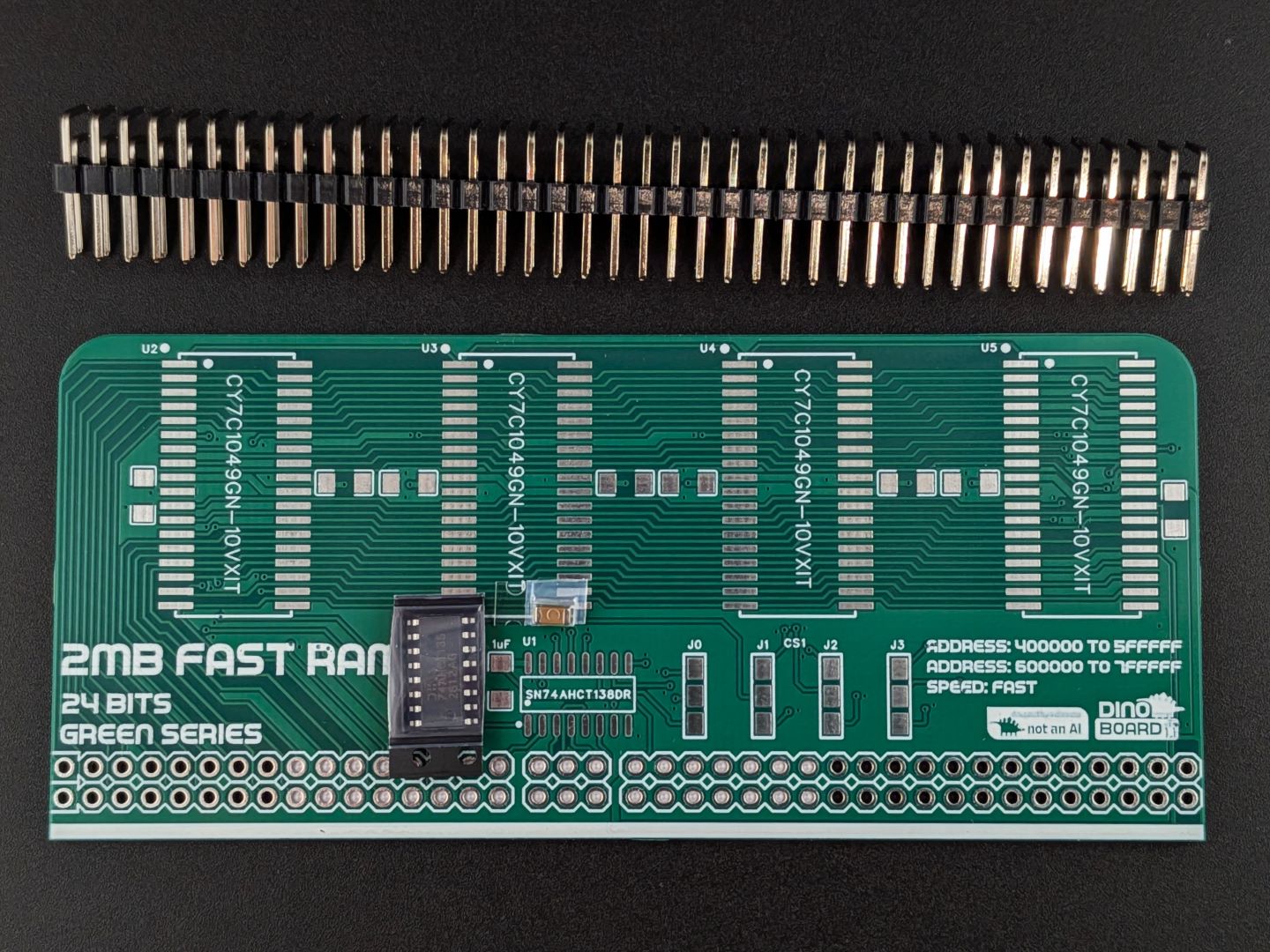 |
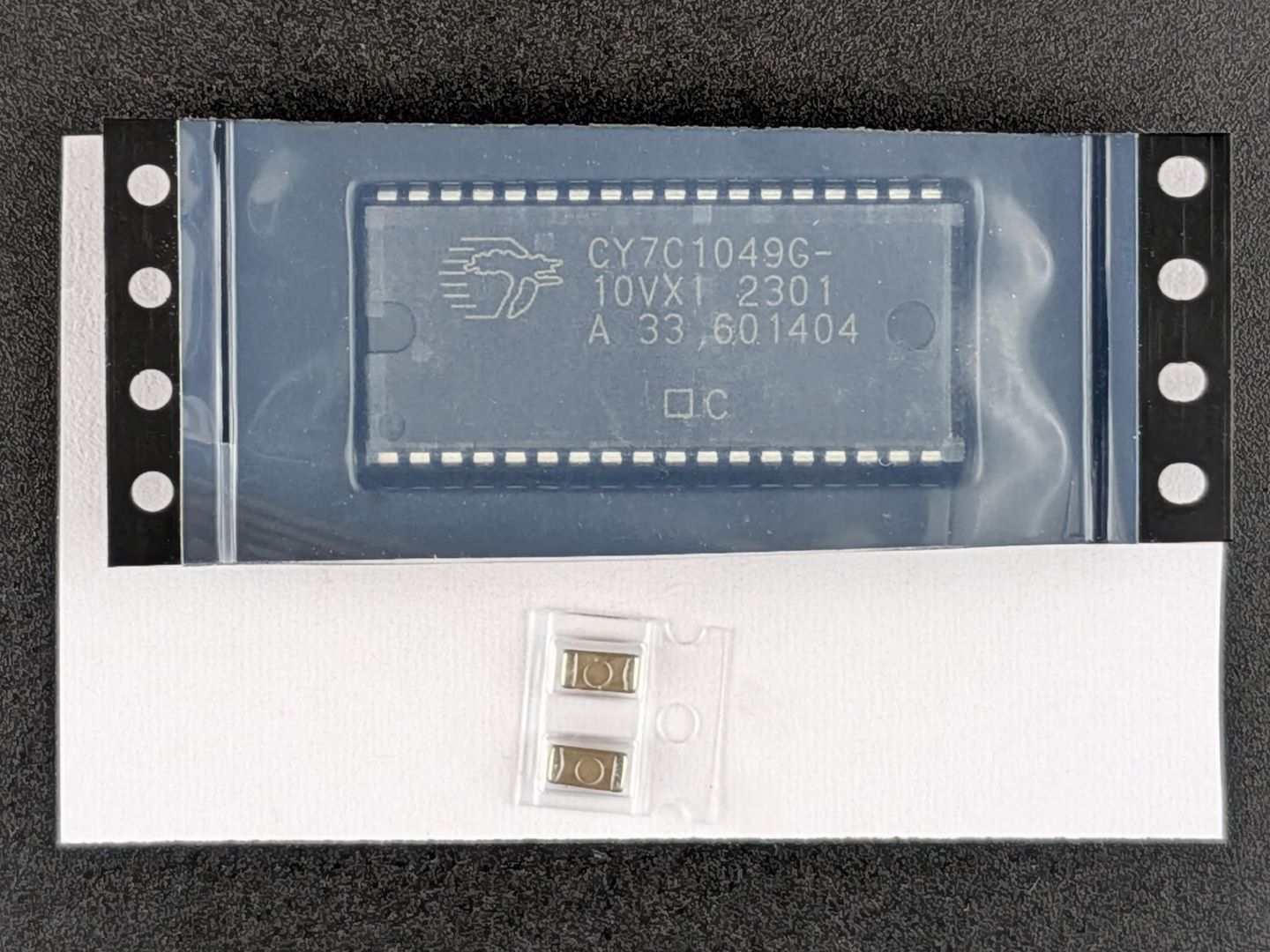 |
There are currently a number of software projects under development to take advantage of this memory module.
* The languages enable the writing of application to take full advantage of the extended memory module. The ports are still under active development. See their respective repos for details of porting progress.
Although it may be possible to use the official Zilog ZDS II development studio to create your own ‘applications’ - this is not a recommended approach.
The EZ80.COM and EXE.COM applications can be downloaded from the one of the official releases on the github repo : https://codeberg.org/dinoboards/ez80-for-rc/releases. Download the releases.zip under the Assets section of the release you want to use. Within that zip file you find the compiled applications. These are standard CP/M applications and will only execute on an eZ80 CPU.
The EZ80.COM CP/M application can be used to verify your memory module is working. Once you have copied it onto your system (typically with xmodem) you can run it to scan, test and adjust the timings of the memory.
Running EZ80.COM with no arguments will report timings:
C>EZ80
              CPU frequency: 25000000 Hz
            Z80 Environment: eZ80's Z80 Compatibility
      On-chip Flash W/S: 1  (80ns)
        Main Memory B/C: 3  (360ns)
Extended Memory CS0 W/S: 2  (120ns)
Extended Memory CS1 W/S: 0  (40ns)
                I/O B/C: 4  (480ns)
         TMR1 Tick rate: 60 (Counter: 218)
To get a list of command line options, run with the -? argument
C>EZ80 -?
Usage: ez80 [options]
Options:
  -F=<number>W      Set On-chip Flash Wait States
  -M=<number>[W|B]  Set Main Memory Wait States or Bus Cycles (CS3)
  -M0=<number>[W|B] Set Extended Memory Wait States or Bus Cycles (CS0)
  -M1=<number>[W|B] Set Extended Memory Wait States or Bus Cycles (CS1)
                    Wait States: 0-7, Bus Cycles: 1-15
  -I=<number>[W|B]  Set I/O Wait States or Bus Cycles (CS2)
  -S                Scan extended memory
  -P                Measure Main Memory Performance
  -T=<number>       Set tick frequency rate (50 or 60)
  -? /?             Show this help message
As shown in the help above, to scan and verify your extended memory is working run with the -S option:
C>EZ80 -S
Searching for memory installed from 0x200000 to 0x7F0000
512K bank at 0x200000: None
512K bank at 0x280000: None
512K bank at 0x300000: None
512K bank at 0x380000: None
512K bank at 0x400000: OK
512K bank at 0x480000: OK
512K bank at 0x500000: OK
512K bank at 0x580000: OK
512K bank at 0x600000: OK
512K bank at 0x680000: OK
512K bank at 0x700000: OK
512K bank at 0x780000: OK

4096kb available at 0x400000

Memory @ 0x400000: 8192.00 KB/s
This kit will include all the required parts for the module (PCB, SMD capacitors, and SMD integrated circuits)
This kit can also be supplied with the SMD parts already soldered for you.
| Quantity | Component | Self Sourcing* |
|---|---|---|
| 5 | 1uF (0805 imperial SMD) | Digikey: CL21B105KOFNNNG |
| 1 | 74AHCT138 (16-SOIC) | Digikey: SN74AHCT138DR |
| 1 to 4 | CY7C1049GN-10VXIT (36-SOJ) | Digikey: CY7C1049GN-10VXIT |
| 2 | Right Angle 2x20 Header | Digikey: 2057-PH2RA-40-UA-ND Mouser: 649-68020-140HLF |
| 1 | PCB |
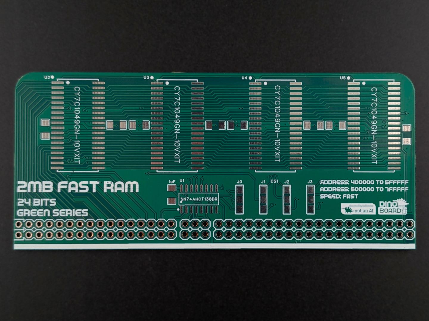
J0 to J3 are pads that need to be bridge to enable a specific memory address operations. The module support 2 memory ranges.
Solder and short the top two pads of each, to configure the memory for address range 0x400000 to 0x05FFFF
And short the bottom two pads of each, to configure the memory for address range 0x060000 to 0x7FFFF
WARNING: Its important not to insert two memory modules into an ozRaptor base configured for the same address range. This will conflict and possible damage the RAM or the eZ80 CPU.
WARNING: Do not short all three pads, as this would also cause operational conflicts.
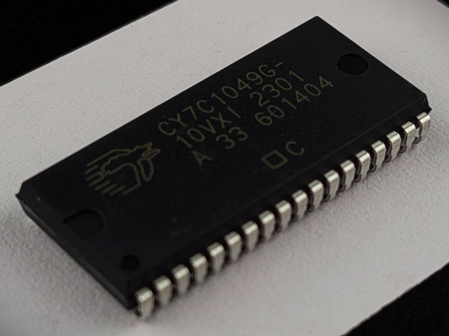
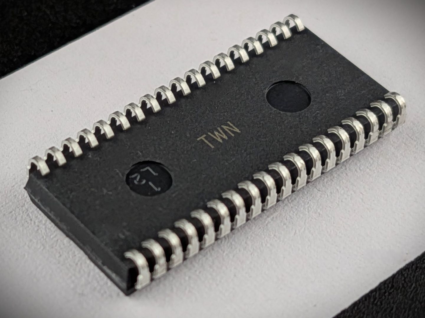
The module can be ordered with all SMD parts soldered. Or if you prefer, you can solder the chips and capacitors yourself.
This module's components are all SMD parts (except for the right hand connector headers).
The SMD parts can be soldered with a conventional soldering iron. If this will be your first attempt to solder SMD components you will need to take your time and pay attention to the points below. (you may wish to practice on a cheap throw away board)
The specific parts have been chosen specifically to assist in visual hand soldering.
Solder each SRAM chip, one at a time, verifying the connections before moving to the next SRAM chip.
After the SRAM chips are done, solder the 74AHCT138 decoder IC.
After all the ICs are done & connection continuity verified, only then proceed with soldering the capacitors.
And finally, solder the 3 set of headers (2x20, 2x3 and 2x16).
The following tools and equipment is recommended:
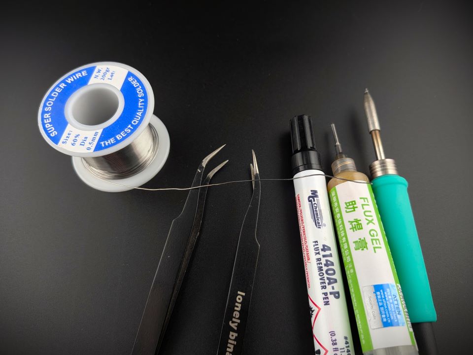
Before starting, clean the PCB using a cleaner such isopropyl alcohol.
On the initial 2 joint soldering, ensure the chip is pushed down against the PCB - otherwise it might ‘float’ a little and prevent a good soldering.
If you get some pins bridging - for the moment, just ignore it - just focus on ensuring the IC is positioned correctly.
There are numerous approached you can use to solder the remaining pins.
Using your multimeter, in continuity mode, check that each pin of the IC are connected to the corresponding pad of the free RAM footprints. Also check that each pin is not shorting with it neighbouring pin.
> When placing a probe on the IC's pin - do not press hard against the pin - as this might give you a false positive if the pin is floating and is not actually soldered.Almost all pins of each IC is connected in parallel. The only pins that are not connected are:
PIN 6 - this pin should connect to the center pad of J0
PIN 36 - (top right pin) is N/C
PIN 19 - (bottom right pin) is also N/C
All other pins should mirror to the other RAM chip's footprint.
If you identify any pins that are not connected - apply some flux and flow a tiny amount of additional solder.
If you identify any bridging - apply some flux and draw excess solder with a clean iron tip.
After each SRAM chip is done & verified, proceed to solder the next item.
Do not fuss if the capacitor is a little wonky. But using your multimeter in continuity mode, confirm the two ends of the capacitor are not shorted. (5V & GND)
Please note that this is a kit, produced by a non-expert (me) for hackers, DIYers’ and retro lovers, to tinker with. Please exercise caution and follow good safety practices. You will be working with sharp knives, a hot soldering iron, and small metal components. Be mindful of the risks involved in the build process. I will do my best to answer any questions you may have.
This kit is provided as-is, with no guarantees or warranties. By assembling and using this kit, you acknowledge that you do so at your own risk.
 Store